Edge Computing
Edge computing is a distributed computing architecture that moves the computing of applications, data and services from the central node of the network to the logical edge nodes of the network for processing.
Edge computing decomposes large services that are originally completely processed by central nodes, cuts them into smaller and more manageable parts and distributes them to edge nodes for processing.
Edge nodes are closer to user terminal devices, which can speed up data processing and transmission and reduce delays. Under this architecture, data analysis and knowledge generation are closer to the source of data, so it is more suitable for processing big data.

The hardware architecture of edge computing primarily consists of three layers:
1. Cloud Layer
Responsible for processing and storing comprehensive data. Even though edge computing aims to reduce reliance on the cloud, cloud computing remains an essential part of the edge computing architecture.
2. Edge Layer
Located between the user and the cloud, it handles real-time data processing to reduce latency and bandwidth usage, thereby increasing response speed.
3. Device Layer
Includes sensors, radio gateways, industrial PCs and embedded computers etc. These devices are deployed at the network edge and are responsible for collecting and generating data.
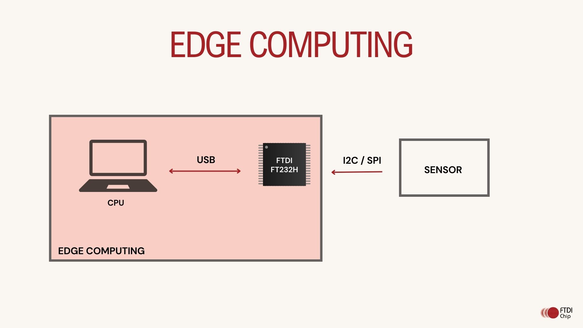
FTDI ICs can be used in the industrial PCs in the device layer to collect information from sensor via I2C or SPI interface.
There are many environment sensors that can be used for collecting environment information. They output data via I2C or SPI interface. However, most PCs only have USB interface to communicate with external devices, hence FTDI products is the ideal solution bridging between the PC and sensors.
The example below uses FTDI’s FT232HL USB to UART IC which has the following key features making it an ideal candidate for a device layer of edge computing device:
-
- Entire USB protocol handled on the chip. No USB specific firmware programming required.
- USB 2.0 Hi-Speed (480Mbits/Second) and Full Speed (12Mbits/Second) compatible.
- Multi-Protocol Synchronous Serial Engine (MPSSE) to simplify synchronous serial protocol (USB to JTAG, I2C, SPI or bit-bang) design.
- FTDI’s royalty-free Virtual Com Port (VCP) and Direct (D2XX) drivers eliminate the requirement for USB driver development in most cases.
- Adjustable receive buffer timeout.
- Option for transmit and receive LED drive signals.
- Highly integrated design includes 5V to 3.3/+1.8V LDO regulator for VCORE, integrated POR function
- Operation configuration mode and USB Description strings configurable in external EEPROM over the USB interface.
- Configurable I/O drives strength (4, 8, 12 or 16mA) and slew rate.
- Low operating and USB suspend current.
- Supports self-powered, bus powered and high-power bus powered USB configurations.
- UHCI/OHCI/EHCI host controller compatible.
- USB Bulk data transfer mode (512 byte packets in Hi-Speed mode).
- +1.8V (chip core) and +3.3V I/O interfacing (+5V Tolerant).
- Extended -40°C to 85°C industrial operating temperature range.
- Compact 48-pin Lead Free LQFP or QFN package
The block diagram below shows at a high level how FTDI’s FT232HL can be integrated into an Edge Computing PC.
Recommended ICs: